 2022-12-17
 The 7408 IC contains four independent two-input AND gates. Each gate produces a logic-high output only when both inputs are high. Its Boolean function is Y = A AND B.
That describes the logic function, but not every electrical requirement. SN7408, SN74LS08, SN74HC08 and SN74HCT08 perform the same basic operation while differing in logic technology, input thresholds, supply requirements and drive characteristics. Those differences matter when building a circuit or replacing an existing device.
7408 truth table
The same truth table applies to each of the four gates. A and B are inputs; Y is the output. Logic 0 and logic 1 mean valid low and high signal levels for the selected device, not necessarily exactly 0 V and the supply voltage.
| Input A | Input B | Output Y |
|---|---|---|
| 0 | 0 | 0 |
| 0 | 1 | 0 |
| 1 | 0 | 0 |
| 1 | 1 | 1 |
7408 pinout: identify the package orientation first
For the conventional 14-pin arrangement, pin 14 is VCC and pin 7 is GND. The four gates use the following connections. Verify the exact manufacturer’s package drawing before wiring or designing a footprint.
- Gate 1: inputs on pins 1 and 2; output on pin 3.
- Gate 2: inputs on pins 4 and 5; output on pin 6.
- Gate 3: inputs on pins 9 and 10; output on pin 8.
- Gate 4: inputs on pins 12 and 13; output on pin 11.
For a 14-pin DIP viewed from above with the notch at the top, pin 1 is at the upper left. Numbering continues down the left side and up the right side. Do not confuse a top-view pin diagram with the underside of the package.
The TI SN7408/SN74LS08 datasheet provides the pin assignments, function table and device-specific electrical limits.
7408, 74LS08, 74HC08 and 74HCT08 are not identical
The “08” function identifies a quad two-input AND gate in these families. The letters between “74” and “08” are important: they identify different logic technologies, not interchangeable marketing names.
- SN7408: standard TTL logic intended for nominal 5 V operation. Use its own supply and loading specifications.
- SN74LS08: low-power Schottky TTL. It shares the AND function but has different electrical characteristics from standard TTL.
- SN74HC08: CMOS logic. TI specifies a 2 V to 6 V operating supply range; its input thresholds must be checked at the chosen supply.
- SN74HCT08: CMOS logic with TTL-compatible input levels, specified by TI for a 4.5 V to 5.5 V operating supply.
A TTL output should not automatically be assumed to meet a 5 V HC input’s guaranteed high-level requirement. HCT can be relevant when TTL-compatible input thresholds are needed, but it still requires a full compatibility check. Consult the official SN74HC08 and SN74HCT08 documentation for the selected variant.
A simple AND-gate connection example
Consider two valid logic signals: ENABLE and REQUEST. Connect ENABLE to gate 1 input A, REQUEST to input B, and read output Y. The output is high only while both inputs are high. This is a basic logic example, not a complete safety interlock or motor-control circuit.
Power the device within its recommended operating range, connect the required ground reference and provide local supply decoupling according to the manufacturer’s guidance. Drive inputs to defined valid levels. Mechanical switches may require pull resistors and debouncing; unused inputs also need appropriate treatment for the selected logic family.
For an initial check, observe the output with a suitable logic probe or oscilloscope. An LED requires current limiting and a check of the gate’s output capability. Do not connect a motor, relay coil or other high-current load directly to a logic output; use an appropriate driver stage and protection.
What to check before approving a replacement
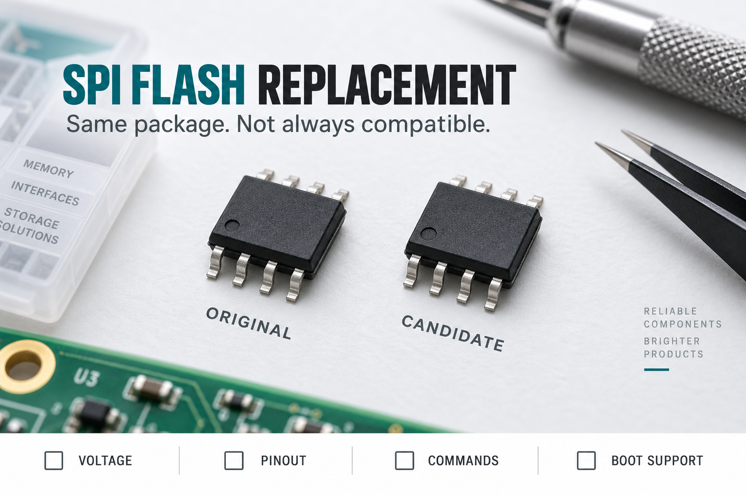
Matching the truth table is only the first step. Compare the following against the existing circuit rather than choosing a replacement solely because its part number ends in “08.”
- Supply and signal levels: confirm recommended supply voltage and guaranteed input/output levels under the actual load.
- Output loading: check source and sink capability, fanout and capacitive loading. Supply current is not the same as output drive current.
- Timing: compare propagation delay and input transition requirements. A different delay can change circuit behavior even when the logic function matches.
- Package and grade: verify footprint, pin assignment, temperature rating and complete ordering suffix.
Do not assign one current-consumption figure or one temperature range to the entire family. Read the specified conditions, distinguish typical values from guaranteed limits, and use recommended operating conditions rather than absolute maximum ratings for normal design.
Common questions about the 7408 IC
Is 7408 an AND gate or a NAND gate?
It is a quad two-input AND-gate device. A NAND gate inverts the AND result and therefore has a different truth table.
Can a 7408 connect directly to a 3.3 V microcontroller?
Not as a blanket rule. Check the exact gate variant, MCU input tolerance and guaranteed signal levels in both directions. A connection that works on one test board may still be outside guaranteed limits.
Can the output be used to gate a clock?
Care is required. An enable signal changing at the wrong time can produce an unwanted pulse. Clock-control applications need timing analysis and may require a dedicated glitch-free clock-gating solution.
Request the complete ordering code, not just “7408”
For a replacement or production enquiry, provide the manufacturer, full part number, package, required quantity and delivery date. State whether you need an exact match or can consider alternatives for engineering approval.
You can search the EASYIEE component catalog or send the marked part number and BOM requirement for a sourcing review. Availability and delivery need confirmation; this guide does not establish stock for any particular variant.
For multiple BOM lines, the OEM component sourcing guide explains how to organize quantities, approved alternatives and acceptance requirements.