 2026-10-12
 MEMORY / TROUBLESHOOTING
SPI flash not detected? First establish whether the chip returns a repeatable, valid JEDEC ID. An all-FF or all-00 result is a diagnostic clue, not proof of a failed chip. Check power, connections, chip select, clocking and the device’s current interface mode. If a valid ID is returned but rejected by software, investigate driver support before replacing the hardware.
This guide focuses on SPI NOR flash used for boot code, firmware and configuration storage. It separates communication failures from identification and replacement problems. NAND flash, eMMC and parallel NOR require different procedures.
What does the JEDEC ID result tell you?
Record the actual received bytes, not just the message “flash not found.” Repeat the read without changing the setup. Stable, unstable and completely absent responses lead to different investigations.
| Observed result | Possible explanation | Next useful check |
|---|---|---|
| JEDEC ID: FF FF FF | The host may be sampling a high or undriven return line; the device may not be responding to this transaction. | Measure power at the chip, then capture CS#, SCK and the return signal at its pins. |
| JEDEC ID: 00 00 00 | The return path may be held low, or the controller may be reading the wrong input or buffer. | Compare the physical signal with the bytes reported by software. |
| ID changes between attempts | Timing, contact, signal integrity or software transfer handling may be inconsistent. | Use a lower supported clock rate and capture repeated transfers. |
| Stable ID, but “unrecognized” | The ID may be unsupported, incorrectly parsed or different from the expected fitted part. | Match raw bytes to the exact datasheet and inspect the installed driver version. |
| Valid ID; memory data is FF | An erased region is one possibility; an incorrect data-read transaction is another. | Verify the read command and address against a region with known contents. |
| Works on a programmer, not on the board | The two setups differ in power, bus ownership, initialization or protocol settings. | Compare both setups rather than assuming the chip is defective. |
Identification is not a memory-content test. Reading an erased data area and reading the identification response are different operations. Linux’s SPI NOR documentation illustrates erased-array reads containing FF; that does not make an all-FF ID a valid identification.
1. Check the exact part, supply and signal levels
Start with the complete ordering code and the correct package drawing. A short marking on the package may not identify every voltage or package variant. Compare the marking with the BOM before choosing a programmer profile.
Measure the supply at the flash power pins while attempting a read. A correct setting on the bench supply does not establish the voltage arriving at the device. Check any separate I/O supply too, and use the manufacturer’s operating range rather than its absolute maximum rating as the target.
Then check the host’s output levels and input thresholds. A voltage adapter must support both power and signal requirements. Our 1.8V vs 3.3V SPI flash comparison explains why changing the supply alone may not make two devices compatible.
At this stage, collect three facts: the exact part fitted, the voltage measured at that part and the voltage domain used by the controller. Keep these in the test record so a later hardware or firmware change can be compared with the same baseline.
2. Verify pin mapping and bus ownership
For a conventional single-data-line SPI connection, check the following paths against the schematic and device pinout:
- Host clock to flash SCK.
- Host chip select to the intended flash CS# or CE#.
- Host transmit data to flash SI / IO0.
- Flash SO / IO1 to the host receive input.
- A shared signal ground and correct package orientation.
Check controller pin multiplexing as well as continuity. A wire can reach the correct pin while firmware configures that pin for a different peripheral. Inspect solder joints or clip contacts with the system unpowered before testing again.
On parts with HOLD# or RESET#, check the documented inactive state. For example, the SST25VF040B datasheet describes HOLD pausing communication and placing its output in a high-impedance state. Do not assume the same physical pin has that role on every flash device; multi-I/O parts can repurpose pins.
When a programmer is attached to a populated board, determine whether the onboard controller can also drive the bus. Do not assume holding the processor in reset guarantees high-impedance pins. Establish one bus master and a documented power arrangement before testing. Check the board’s programming instructions rather than connecting two power sources by trial and error.
3. Capture a complete Read ID transaction
A successful SPI API call only means the controller completed what it was asked to do. It does not prove the flash received the intended command. Capture signals close to the flash and compare the transaction with its datasheet.
Use a conservative clock rate supported by the device and controller. Confirm bit order, clock polarity and phase, bus width, command framing and received-byte alignment. Inspect an actual capture before changing multiple settings at once.
- 01CE# lowSelect the device
- 02Send 9Fh8 command clocks
- 03Read BF 25 8D24 response clocks
- 04CE# highEnd the transaction
Logical sequence only, not a measured waveform. The expected bytes are specific to this device.
The Microchip/SST Read-ID specification, page 20 defines this example without an address phase. Do not add a memory address simply because a data-read routine normally uses one. Do not apply this example unchanged to another family: the Infineon CYRS17B512 datasheet, section 8.2.1, for instance, specifies dummy cycles for its RDID transaction.
Keep chip select active for the entire command and response, and release it only after the peripheral has finished clocking. In an Infineon support discussion about failed ID reads, support specifically investigated manually controlled chip select and requested a logic-analyzer trace. This is a useful diagnostic example, not evidence that every failed read has that cause.
4. Check startup, reset and SPI versus QPI mode
The host and flash must agree on how commands are transmitted. A flash configured for four-line QPI command input may not interpret a one-line SPI command. A microcontroller reset also does not necessarily reset a separately powered flash.
Infineon’s legacy SPI command guidance for QPI mode explains this mismatch for the covered devices. Check your own part’s supported modes and documented recovery sequence. “Quad read” does not automatically mean every command is sent on four lines.
Review power-up wait times, deep-power-down release if supported, and reset completion requirements. Do not send a guessed reset sequence or rewrite nonvolatile configuration registers as a generic fix. Record the current configuration where it can be read, then make one documented change at a time.
If detection fails only after a warm reset, compare the flash’s state before and after that reset. If it fails only at higher speed, return to timing and electrical measurements. These comparisons narrow the investigation without treating the chip as the only possible fault.
5. If the ID is valid, check driver and programmer support
A repeatable ID that matches the fitted device shows that identification communication is working under the tested conditions. It does not yet validate normal reads, writes or boot operation.
Record the controller, software version, raw ID bytes and expected device. Check whether that version supports the flash and whether it parses the returned byte order and length correctly. Replacing a component with a newer device can expose a software support gap even when the electrical connection is sound.
The Linux SPI NOR framework documentation explains how SFDP tables describe device capabilities. Some flashes work through generic SFDP probing; others need explicit entries or fixes. A similar capacity or matching manufacturer byte is not enough to choose an arbitrary device profile.
Keep initial investigation read-only. Do not force an erase or programming operation to bypass an identification error. Once detection is reliable, back up recoverable data and use an approved test area for any subsequent write validation.
What if detection failed after replacing the flash?
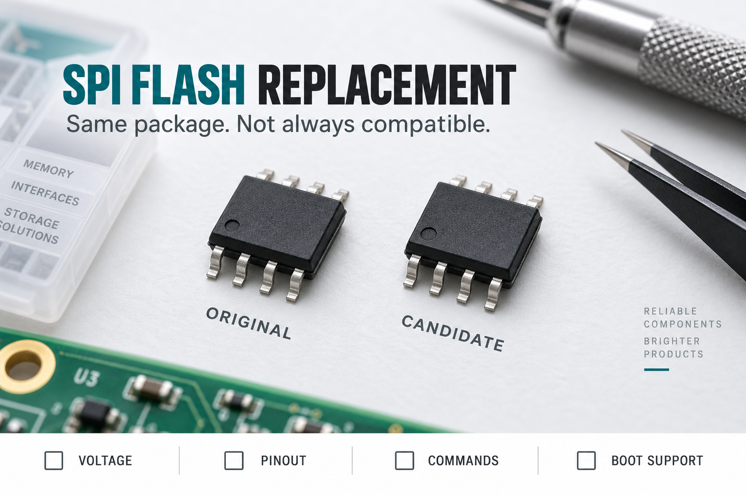
Write down the old and new complete part numbers side by side. First compare voltage, package and pinout; then review command formats, startup state, reset behavior and driver recognition. Continue with addressing, erase layout and boot compatibility after identification works.
Use the SPI flash replacement compatibility checklist to organize that review. Passing the ID check is one checkpoint, not approval of the replacement for production.
For example, a board may recognize the new flash but still fail to boot because its boot sequence expects a different read configuration. Keep “device detected,” “firmware read successfully” and “system boot validated” as separate results in the engineering report.
A useful record for the next engineer
A short, repeatable test record is more valuable than “tried several chips.” Capture the details below before escalating a failure:
Exact flash ordering code:
Board and controller:
Driver / programmer version:
Supply measured at flash pins:
SPI clock and interface mode:
Command and raw received bytes:
Cold-start result / warm-reset result:
Logic-analyzer capture filename:
One change made and its result:
Label hypothetical explanations as hypotheses until a measurement supports them. If the fault remains, this record helps hardware and firmware engineers decide the next experiment without repeating your work.
Frequently asked questions
Does a JEDEC ID of 0xFFFFFF mean the flash is dead?
No. That response alone cannot identify the fault. Establish that the device is powered correctly, receives the right transaction and can drive the return path before concluding that the chip has failed.
Why does SPI flash return 0x000000?
Investigate a low return signal, pin mapping and receive-buffer handling. Compare the signal captured at the flash with the software result; zeros in a buffer do not prove zeros were transmitted by the device.
Can a blank flash still return a JEDEC ID?
Yes. On devices implementing JEDEC Read ID, identification is separate from user firmware contents. A blank memory array does not by itself explain a missing valid identification response.
Can the same chip work on a programmer but fail in circuit?
Yes. The programmer and board can differ in supply, bus loading, startup state, clock rate and software support. Compare those conditions before replacing the device again.
Should I erase the flash to fix an identification error?
No. Erasing firmware is not a first-line remedy for a communication or recognition failure. Resolve detection first and preserve recoverable contents before any authorized write or erase test.
Need to source the confirmed flash part?
Once engineering has identified the required device, prepare the complete ordering code, manufacturer, quantity and delivery date. State whether the request is for an exact match or an alternative awaiting approval. The SPI NOR flash sourcing guide covers the purchasing details.
Send EASYIEE your part requirement or BOM to request availability and a quotation. Include the proposed replacement separately so it is not mistaken for an approved substitute.
Technical basis: manufacturer documentation and the Linux SPI NOR documentation linked beside the relevant explanations. The sequence diagram is illustrative; no bench measurement or product qualification is claimed.