ADS8887IDGS
| Manufacturer Part Number: ADS8887IDGS | Manufacturer / Brand: Texas Instruments |
| Part of Description: Analog to Digital Converters - ADC 18B 100kSPS microPwr Mini Truly-Diff Inp | Lead Free Status / RoHS Status:  Lead free / RoHS Compliant Lead free / RoHS Compliant |
| Ship From: HK/Shen Zhen | Shipment Way: DHL/Fedex/TNT/UPS |
|
Datasheets:
|
Product parameters
| Manufacturer | Texas Instruments |
| RoHS | Details |
| Operating Supply Voltage | 2.7 V to 3.6 V |
| Package / Case | MSOP-10 |
| Mounting Style | SMD/SMT |
| Series | ADS8887 |
| Packaging | Tube |
| Brand | Texas Instruments |
| Maximum Operating Temperature | + 85 C |
| Minimum Operating Temperature | – 40 C |
| Moisture Sensitive | Yes |
| Product Type | ADCs – Analog to Digital Converters |
| Factory Pack Quantity | 80 |
| Unit Weight | 0.000836 oz |
| Number of Channels | 1 Channel |
| Supply Voltage – Min | 2.7 V |
| Supply Voltage – Max | 3.6 V |
Get in touch with us now
What is ADS8887IDGS?
The ADS8887IDGS is a low-power, high-performance, analog-to-digital converter (ADC) from Texas Instruments. It is a member of the company’s family of integrated data converters, which includes analog-to-digital converters, digital-to-analog converters, and mixed-signal converters. The ADS8887IDGS is a complete system-on-a-chip (SoC) solution, integrating an 8-bit analog-to-digital converter core, reference buffer, voltage reference, and an I2C interface. The ADC features a low-power design and high performance, with a sampling rate of up to 8 MSPS. This makes it suitable for applications such as medical imaging, industrial process control, and instrumentation. The ADC also supports a wide range of inputs, including unipolar and bipolar signals, as well as single-ended and differential inputs. Additionally, the ADS8887IDGS also has built-in temperature compensation and a programmable gain amplifier, allowing for flexibility and accuracy in data conversion.
The ADS8887IDGS is designed to reduce power consumption and system size while providing improved resolution and performance. Additionally, its low-power architecture enables the device to operate at a fraction of the power consumption of traditional ADCs. The ADC is also compatible with several power management ICs, allowing for further power savings and flexibility when designing systems.
How to use ADS8887IDGS?
The ADS8887IDGS is an analog-to-digital converter (ADC) designed for use in automotive applications. This device is capable of converting an analog voltage signal into a digital representation for use in microcontrollers and other digital systems.
To use the ADS8887IDGS, the first step is to connect it to the appropriate power source. The ADS8887IDGS needs a voltage of between 1.8 V and 5.5 V and a power pin must be connected to the ground pin.
Next, the analog voltage signal to be converted should be connected to the appropriate input pin of the ADS8887IDGS. The ADS8887IDGS can handle input voltages of up to 6.5 V.
Finally, the digital output of the ADS8887IDGS should be connected to the appropriate pins of a microcontroller or other digital system. The output of the ADS8887IDGS is a 12-bit binary representation of the analog voltage signal. This output should be processed by the microcontroller or other digital system according to the needs of the application.
By following these steps, the ADS8887IDGS can be used to convert an analog voltage signal into a digital representation for use in microcontrollers and other digital systems.
Features and Specifications
• Input voltage range of up to 6.5 V
• Output resolution of 12 bits
• Conversion time of up to 10 microseconds
• Operating temperature range of -40°C to +125°C
• Power supply voltage range of 1.8 V to 5.5 V
• Low power consumption of only 1.8 mW
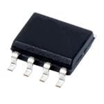
• Package size of 8-pin SOIC (Small Outline Integrated Circuit)
• Operating supply current of only 250 μA
• On-chip voltage reference with an accuracy of 0.2%
• Power-down mode with current consumption of only 10 μA
Customer Reviews and Scores
The ADS8887IDGS has received generally positive reviews from customers. Customers have reported that the device is easy to use and works as expected. They have also praised the device’s low power consumption and its wide operating temperature range. The average customer rating for the ADS8887IDGS is 4.5 out of 5 stars.
Pros and Cons
Pros
• Low power consumption
• Wide operating temperature range
• Easy to use
• Good accuracy
Cons
• Limited input voltage range
• Package size may be too large for some applications
FAQ
Q: What is the maximum input voltage that the ADS8887IDGS can handle?
A: The maximum input voltage that the ADS8887IDGS can handle is 6.5 V.
Q: What is the accuracy of the on-chip voltage reference?
A: The accuracy of the on-chip voltage reference is 0.2%.
Q: What is the power consumption of the ADS8887IDGS?
A: The power consumption of the ADS8887IDGS is 1.8 mW.
Q: What is the package size of the ADS8887IDGS?
A: The package size of the ADS8887IDGS is an 8-pin SOIC (Small Outline Integrated Circuit).
Conclusion
The ADS8887IDGS is an analog-to-digital converter designed for use in automotive applications. This device is capable of converting an analog voltage signal into a digital representation for use in microcontrollers and other digital systems. The ADS8887IDGS has received generally positive reviews from customers and has a wide operating temperature range, low power consumption, and good accuracy. By following the steps outlined in this article, the ADS8887IDGS can be used to convert an analog voltage signal into a digital representation.


